Project
Automotive CAN Telemetry System
ESP32-based automotive telemetry platform developed from a two-node CAN bench network into a custom CAN interface PCB. Bench-tested CAN transmission and reception with live TFT telemetry, then designed a 2-layer SN65HVD230 transceiver board with switchable termination, ground-plane routing, antenna keepout, and electrical DRC validation for future Porsche Taycan integration.
I built this project to learn how embedded systems communicate in an automotive environment and to work toward safely reading telemetry from a Porsche Taycan.
Rather than beginning on a real vehicle network, I first created an isolated two-node CAN bench system using ESP32 microcontrollers and CAN transceivers. This gave me a controlled environment for testing the physical CAN bus, developing firmware, debugging communication, and validating the system before attempting vehicle integration.
After establishing reliable CAN communication and integrating a TFT telemetry display, I translated the breadboard prototype into a custom 2-layer CAN interface PCB in Altium Designer.
Project Goal
Build a reusable embedded interface capable of receiving automotive CAN traffic, processing useful telemetry, and presenting it on a standalone display while developing and validating the system safely on the bench before connection to a vehicle.
System Architecture
The development setup uses two ESP32 nodes connected through SN65HVD230 CAN transceivers. One node can generate traffic while the second receives and processes it, allowing the entire communication path to be tested without relying on a vehicle ECU.
ESP32 Node A
      │
     TWAI
      │
 SN65HVD230
      │
 CANH / CANL
      │
 SN65HVD230
      │
     TWAI
      │
 ESP32 Node B
      │
     TFT
Development Process
Built a two-node CAN bench network
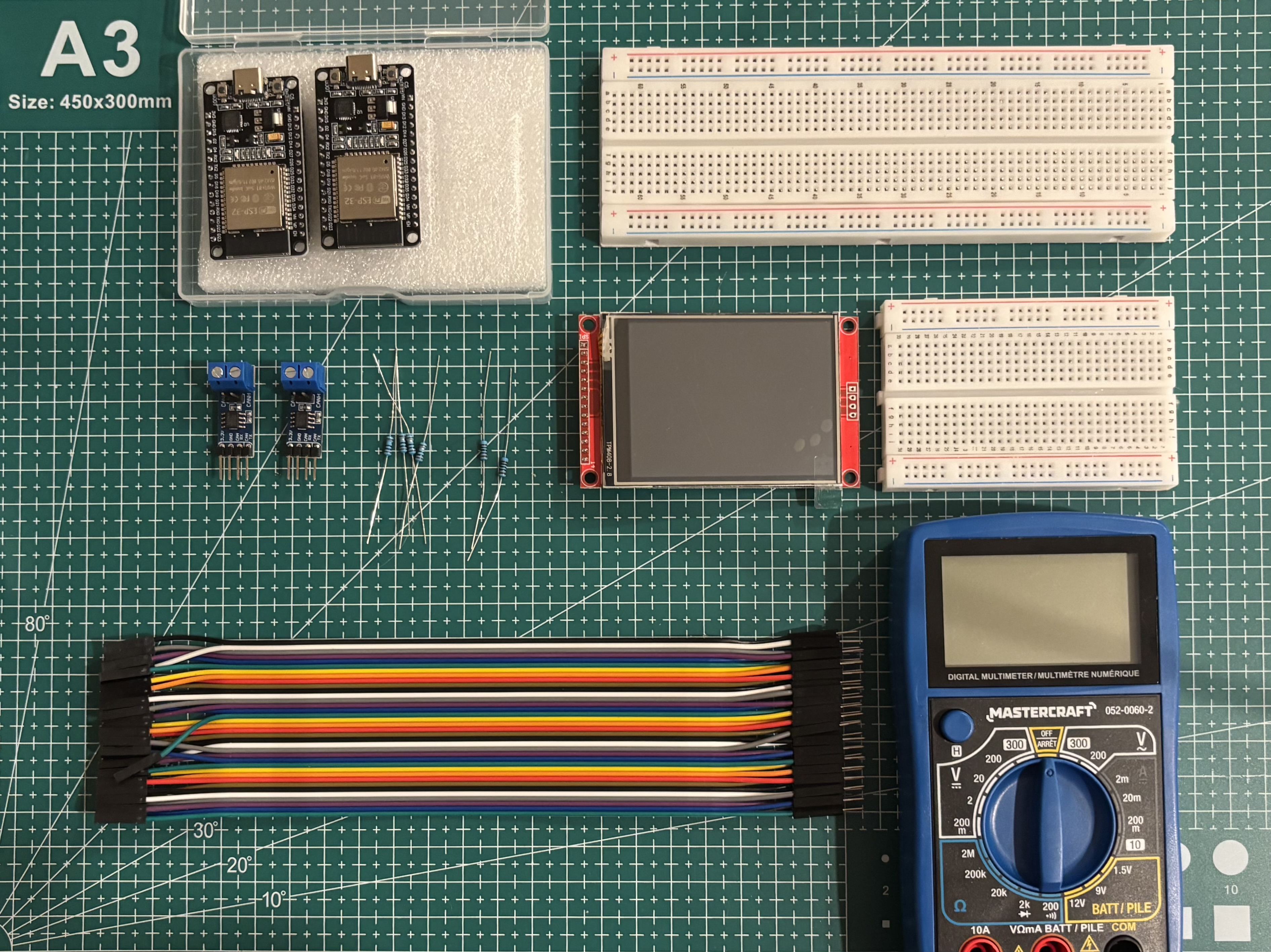
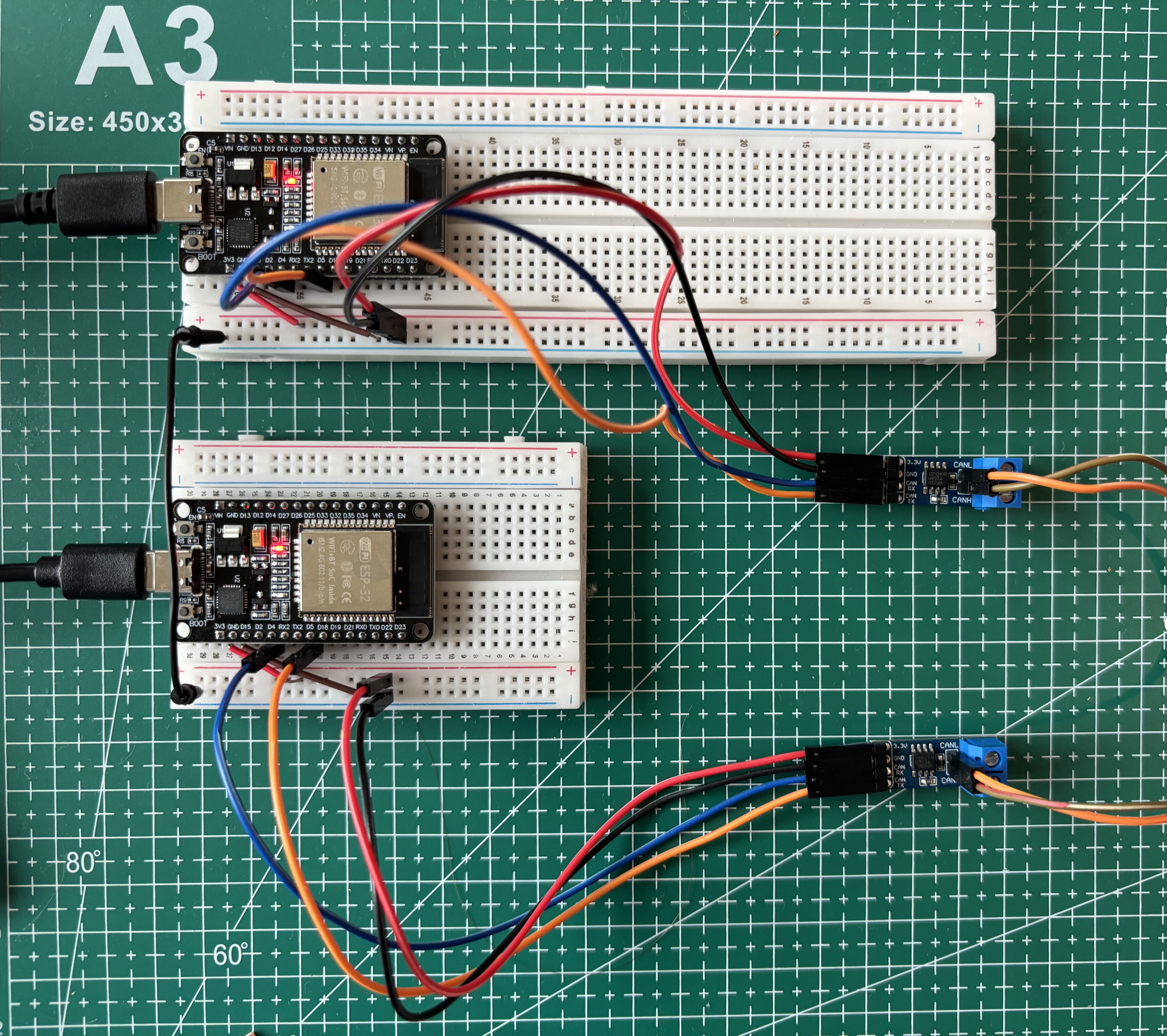
I started with two ESP32 development boards and two SN65HVD230 CAN transceiver modules. CANH and CANL connected the nodes, both systems shared a common ground, and the bus was terminated with 120 Ω resistors.
Debugged the physical CAN bus
Initial transmission attempts failed, so I verified power, grounding, transceiver connections, bus termination, and the presence of a second active CAN node. I used a multimeter to confirm the termination resistance across CANH and CANL.
Implemented ESP32 CAN communication
I configured the ESP32 built-in TWAI controller in Embedded C++ and successfully transmitted and received CAN frames between the two nodes. The final interface uses GPIO5 for CAN TX and GPIO4 for CAN RX.
Integrated a TFT display
I added an SPI TFT display to the receiving ESP32 so CAN data could be processed and displayed as a real-time telemetry interface.
Translated the prototype into a schematic
After validating the CAN interface on the bench, I recreated the hardware in Altium Designer around an ESP32 DevKit and SN65HVD230 CAN transceiver.
Designed the custom PCB
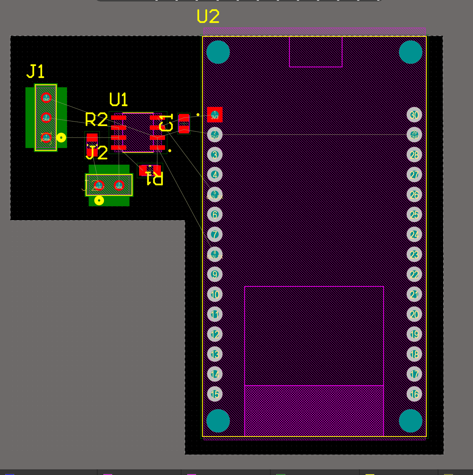
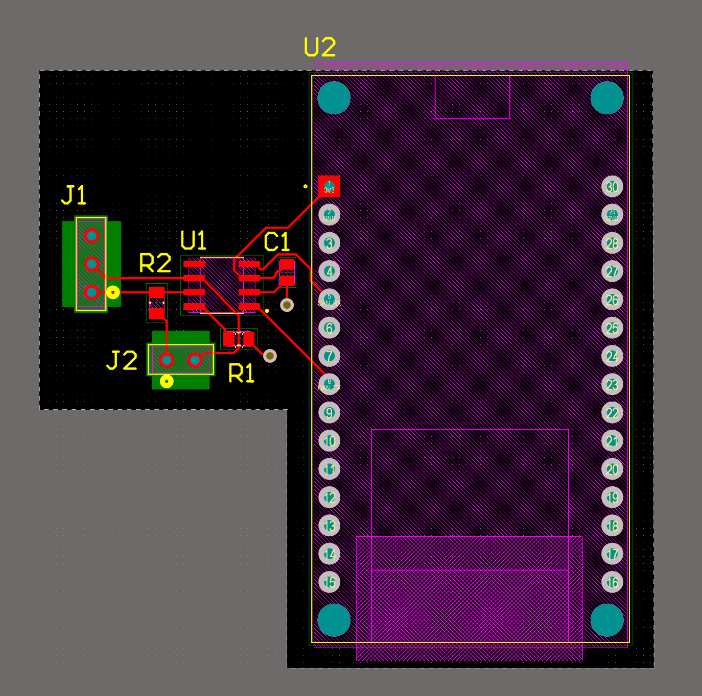
I assigned footprints, synchronized the schematic and PCB, positioned the CAN circuitry around the ESP32, created a compact L-shaped carrier board, and manually routed the design.
Added grounding and RF considerations
The PCB uses a bottom-layer GND polygon with local ground vias for the SMD circuitry. I also added a copper, track, and via keepout beneath the ESP32 antenna region.
Validated the PCB design
I ran Altium Design Rule Checks and resolved connectivity, routing, via assignment, and hole-size issues. The final board passes all electrical routing and connectivity checks, with four remaining silkscreen-to-solder-mask clearance violations on an imported resistor footprint that do not affect electrical functionality.
Bench Prototype
The first version of the system used two ESP32 development boards, two SN65HVD230 transceiver modules, breadboards, and discrete 120 Ω termination. Building both sides of the CAN network meant I could control the traffic being transmitted and test the receiver independently of a real ECU.
Initial transmission failures became an important debugging exercise. I checked the complete hardware chain rather than treating the problem as purely software: common ground, transceiver power, CANH and CANL continuity, termination resistance, firmware configuration, and GPIO assignments.
Embedded Software
Firmware is written in C++ using the ESP32's built-in TWAI controller. The bench implementation configures the CAN controller, transmits frames from one node, receives messages on the second node, and exposes received values to the TFT interface.
Custom CAN Interface PCB
Once the CAN interface had been validated on the bench, I translated the circuit into a custom 2-layer carrier PCB designed in Altium Designer.
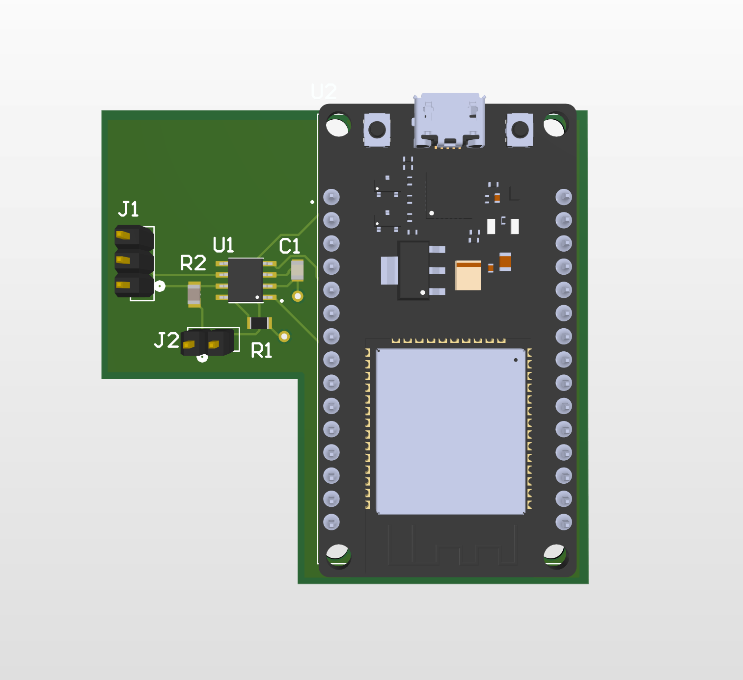
The board is built around an ESP32 DevKit and an SN65HVD230DR 3.3 V CAN transceiver. The CAN circuitry is positioned close to the relevant ESP32 GPIO pins while the external CAN connector is placed at the outside edge for accessibility.
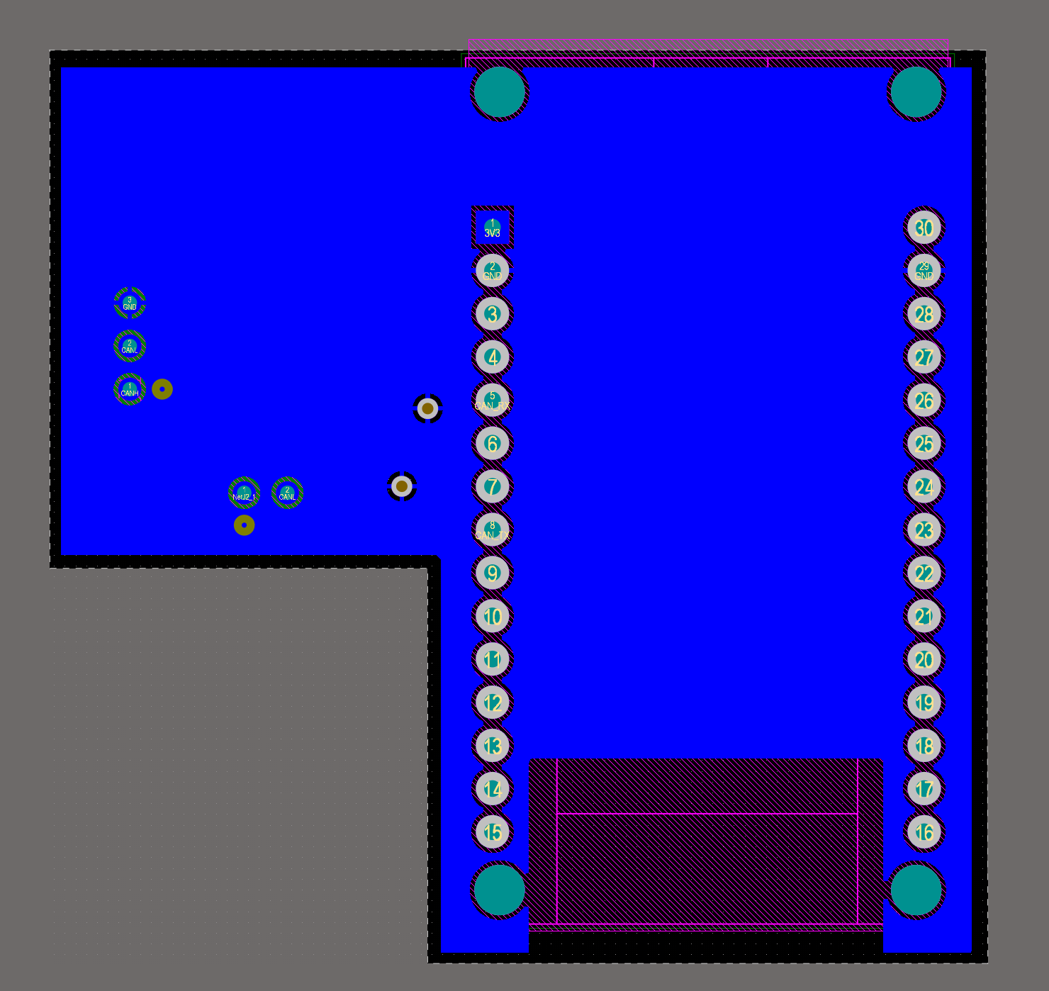
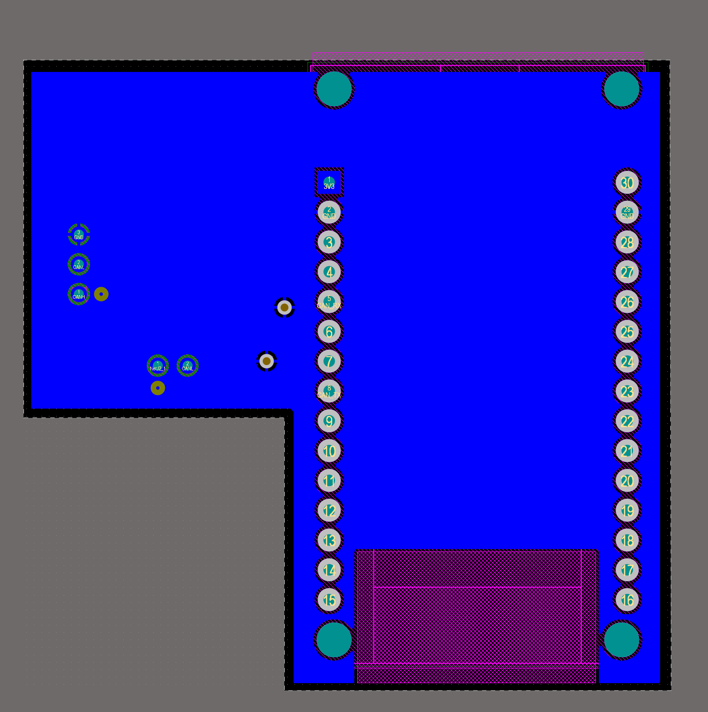
Ground Plane & Antenna Keepout
The bottom layer is used as a GND polygon to provide a broad return path across the carrier board. Under the ESP32 antenna, copper, tracks, and vias are intentionally excluded with a keepout region.
Switchable CAN Termination
CAN buses require 120 Ω termination at the physical ends of the network, but a diagnostic interface should not always add another termination resistor.
I therefore designed the PCB with an optional termination path. R2 provides the 120 Ω resistance and J2 acts as the enable jumper. Installing the jumper completes the path between CANH and CANL; removing it leaves the termination disconnected.
Engineering Decisions
Bench first, vehicle second
The communication system was developed on an isolated two-node CAN network before any connection to the vehicle.
3.3 V transceiver
The SN65HVD230 provides a CAN physical-layer interface compatible with the ESP32 logic level.
Optional CAN termination
A jumper-selectable 120 Ω resistor allows the board to be used either at a bus endpoint or on an already-terminated network.
Bottom ground plane
A bottom-layer GND polygon provides a continuous return path while local vias connect the top-layer SMD ground nodes.
ESP32 antenna keepout
Copper, vias, and tracks are excluded beneath the antenna region to avoid unnecessarily degrading RF performance.
L-shaped carrier PCB
The board outline removes unused material while maintaining component clearance, connector access, and ESP32 USB accessibility.
PCB Debugging & Validation
PCB development involved more than routing traces. I worked through footprint-library issues, schematic-to-PCB synchronization, incorrect pin mappings, an unassigned ground via, mechanical-hole rules, silkscreen conflicts, polygon connectivity, and antenna keepout configuration.
The final design passes Altium's key electrical and manufacturing checks with zero clearance violations, zero short-circuits, zero unrouted nets, zero trace-width violations, and zero hole-size violations.
Four cosmetic silkscreen-to-solder-mask warnings remain on the imported R1 resistor footprint. They do not affect electrical connectivity or board function.
Validation
Final PCB
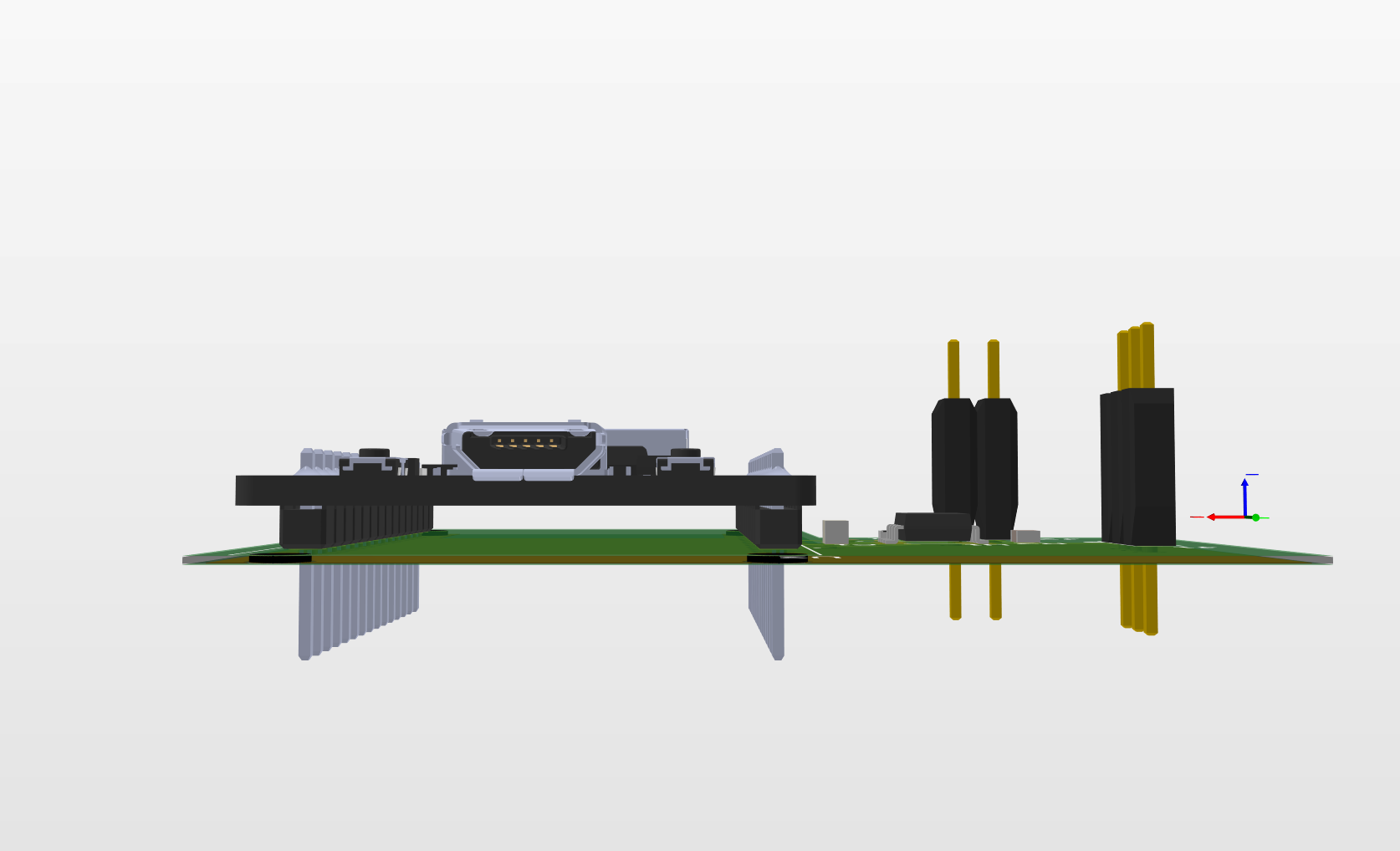
The final 3D review was used to inspect component orientation, connector accessibility, ESP32 fit, USB clearance, and the mechanical relationship between the DevKit and carrier board.
What I Learned
This project moved me beyond treating CAN as only a software protocol. Building the entire system required considering the physical and embedded layers together: differential signaling, termination, transceiver behavior, grounding, GPIO mapping, decoupling, footprints, PCB routing, manufacturing rules, and mechanical accessibility.
It was also my first time taking an embedded prototype from a breadboard implementation through schematic capture, custom PCB layout, design-rule validation, ground-plane design, and final 3D mechanical review in Altium Designer.
Current Status
The two-node CAN bench network, ESP32 CAN communication, TFT integration, schematic, and custom PCB design are complete.
The PCB has not been fabricated and the system has not yet been connected to the Porsche Taycan. Vehicle-specific diagnostic communication remains a future phase.
Next Steps
- • Implement UDS diagnostic request / response
- • Add ISO-TP multi-frame transport
- • Research Taycan-specific diagnostic identifiers
- • Perform safe read-only vehicle integration
- • Decode real vehicle telemetry
- • Fabricate and bench-test the custom PCB